- 您现在的位置:买卖IC网 > Sheet目录447 > IRFW630BTM_FP001 (Fairchild Semiconductor)MOSFET N-CH 200V 9A D2PAK
�� �
�
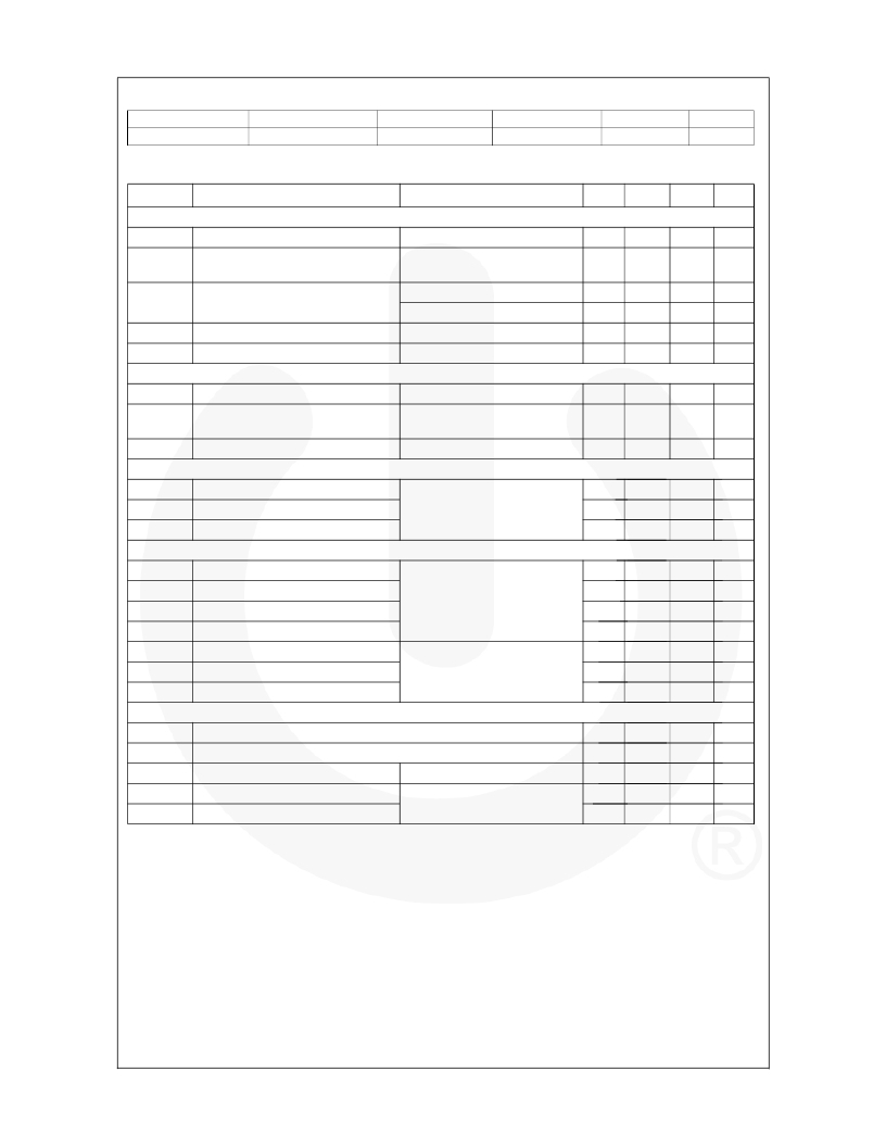
�Package� Marking� and� Ordering� Information�
�Device� Marking�
�IRFW630B�
�Device�
�IRFW630BTM_FP001�
�Package�
�D� 2� -PAK�
�Reel� Size�
�330� mm�
�Tape� Width�
�24� mm�
�Quantity�
�800� units�
�Electrical� Characteristics�
�T� C� =� 25°C� unless� otherwise� noted� .�
�Symbol�
�Parameter�
�Conditions�
�Min�
�Typ�
�Max�
�Unit�
�Off� Characteristics�
�BV� DSS�
�?� BV� DSS�
�/� ?� T� J�
�I� DSS�
�I� GSSF�
�I� GSSR�
�Drain-Source� Breakdown� Voltage�
�Breakdown� Voltage� Temperature�
�Coefficient�
�Zero� Gate� Voltage� Drain� Current�
�Gate-Body� Leakage� Current,� Forward�
�Gate-Body� Leakage� Current,� Reverse�
�V� GS� =� 0� V,� I� D� =� 250� μ� A�
�I� D� =� 250� μ� A,� Referenced� to� 25� °� C�
�V� DS� =� 2� 00� V,� V� GS� =� 0� V�
�V� DS� =� 16� 0� V,� T� C� =� 125� °� C�
�V� GS� =� 30� V,� V� DS� =� 0� V�
�V� GS� =� -30� V,� V� DS� =� 0� V�
�2� 00�
�--�
�--�
�--�
�--�
�--�
�--�
�0.� 2�
�--�
�--�
�--�
�--�
�--�
�--�
�10�
�100�
�100�
�-100�
�V�
�V� /� ο� C�
�μ� A�
�μ� A�
�nA�
�nA�
�On� Characteristics�
�V� GS(th)�
�R� DS(on)�
�g� FS�
�Gate� Threshold� Voltage�
�Static� Drain-Source�
�On-Resistance�
�Forward� Transconductance�
�V� DS� =� V� GS� ,� I� D� =� 250� μ� A�
�V� GS� =� 10� V,� I� D� =� 4.� 5� A�
�V� DS� =� 40� V,� I� D� =� 4.� 5� A�
�2.0�
�--�
�--�
�--�
�0.� 34�
�7.05�
�4.0�
�0.� 4�
�--�
�V�
�?�
�S�
�Dynamic� Characteristics�
�C� iss�
�C� oss�
�C� rss�
�Input� Capacitance�
�Output� Capacitance�
�Reverse� Transfer� Capacitance�
�V� DS� =� 25� V,� V� GS� =� 0� V,�
�f� =� 1.0� MHz�
�--�
�--�
�--�
�550�
�85�
�22�
�720�
�110�
�2� 9�
�pF�
�pF�
�pF�
�Switching� Characteristics�
�t� d(on)�
�t� r�
�t� d(off)�
�t� f�
�Q� g�
�Q� gs�
�Q� gd�
�Turn-On� Delay� Time�
�Turn-On� Rise� Time�
�Turn-Off� Delay� Time�
�Turn-Off� Fall� Time�
�Total� Gate� Charge�
�Gate-Source� Charge�
�Gate-Drain� Charge�
�V� DD� =� 10� 0� V,� I� D� =� 9.0� A�
�R� G� =� 25� ?�
�V� DS� =� 16� 0� V,� I� D� =� 9.0� A�
�V� GS� =� 10� V�
�(Note� 4)�
�(Note� 4)�
�--�
�--�
�--�
�--�
�--�
�--�
�--�
�11�
�70�
�60�
�65�
�22�
�3.6�
�10.2�
�30�
�1� 5� 0�
�130�
�140�
�29�
�--�
�--�
�ns�
�ns�
�ns�
�ns�
�nC�
�nC�
�nC�
�Drain-Source� Diode� Characteristics� and� Maximum� Ratings�
�I� S�
�I� SM�
�Maximum� Continuous� Drain-Source� Diode� Forward� Current�
�Maximum� Pulsed� Drain-Source� Diode� Forward� Current�
�--�
�--�
�--�
�--�
�9.0�
�36�
�A�
�A�
�V� SD�
�t� rr�
�Q� rr�
�Drain-Source� Diode� Forward� Voltage�
�Reverse� Recovery� Time�
�Reverse� Recovery� Charge�
�V� GS� =� 0� V,� I� S� =� 9.0� A�
�V� GS� =� 0� V,� I� S� =� 9.0� A�
�dI� F� /dt� =100� A/� μ� s�
�--�
�--�
�--�
�--�
�140�
�0.87�
�1.� 5�
�--�
�--�
�V�
�ns�
�μ� C�
�Notes:�
�1.� Repetitive� r� ating:� p� ulse� -� width� limited� by� maximum� junction� temperature� .�
�2.� L� =� 3� mH,� I� AS� =� 9.0� A,� V� DD� =� 50� V,� R� G� =� 25� ?,� s� tarting� T� J� =� 25°C� .�
�3.� I� SD� ≤� 9.0� A,� di/dt� ≤� 3� 00� A/� μ� s,� V� DD� ≤� BV� DSS,� s� tarting� T� J� =� 25°C� .�
�4� .� Essentially� i� ndependent� of� o� perating� t� emperature� .�
�?200� 2� Fairchild� Semiconductor� Corporation�
�IRFW630B� Rev.� C1�
�2�
�www.fairchildsemi.com�
�发布紧急采购,3分钟左右您将得到回复。
相关PDF资料
IRFZ14STRR
MOSFET N-CH 60V 10A D2PAK
IRFZ24NSTRR
MOSFET N-CH 55V 17A D2PAK
IRFZ24STRRPBF
MOSFET N-CH 60V 17A D2PAK
IRFZ34E
MOSFET N-CH 60V 28A TO-220AB
IRFZ34NL
MOSFET N-CH 55V 29A TO-262
IRFZ34STRLPBF
MOSFET N-CH 60V 30A D2PAK
IRFZ44ESTRL
MOSFET N-CH 60V 48A D2PAK
IRFZ44E
MOSFET N-CH 60V 48A TO-220AB
相关代理商/技术参数
IRFW634A
制造商:未知厂家 制造商全称:未知厂家 功能描述:TRANSISTOR | MOSFET | N-CHANNEL | 250V V(BR)DSS | 8.1A I(D) | TO-263AB
IRFW634B
制造商:FAIRCHILD 制造商全称:Fairchild Semiconductor 功能描述:250V N-Channel MOSFET
IRFW634BTM_FP001
功能描述:MOSFET RoHS:否 制造商:STMicroelectronics 晶体管极性:N-Channel 汲极/源极击穿电压:650 V 闸/源击穿电压:25 V 漏极连续电流:130 A 电阻汲极/源极 RDS(导通):0.014 Ohms 配置:Single 最大工作温度: 安装风格:Through Hole 封装 / 箱体:Max247 封装:Tube
IRFW634BTMFP001
制造商:Rochester Electronics LLC 功能描述:- Bulk
IRFW640
制造商:FAIRCHILD 制造商全称:Fairchild Semiconductor 功能描述:200V N-Channel MOSFET
IRFW640A
制造商:未知厂家 制造商全称:未知厂家 功能描述:TRANSISTOR | MOSFET | N-CHANNEL | 200V V(BR)DSS | 18A I(D) | TO-263AB
IRFW640B
制造商:FAIRCHILD 制造商全称:Fairchild Semiconductor 功能描述:200V N-Channel MOSFET
IRFW640BTM
制造商:Rochester Electronics LLC 功能描述: 制造商:Fairchild Semiconductor Corporation 功能描述: